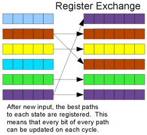
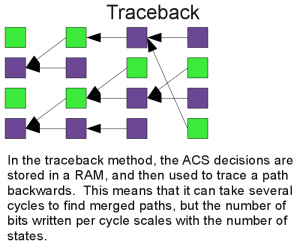
There are two basic ways to keep track of the best path to get to each state. These are the register-exchange, and the traceback method. The register exchange is very easy to understand, and works well for small constraint lengths. The traceback method is a bit more difficult, but works well for longer constraint length codes.
The register exchange method is fairly basic — each state has an N bit register associated with it. The best path is loaded into this register each cycle. This largely prevents the use of RAM. At the same time, the best path data is very easy to access. For a 7b constraint length, this would mean 128 registers with at least 42b each, which is a considerable amount of registers.
The traceback method stores the decisions from the ACS into a RAM. Later, the decisions are read out. The best path is determined by reading backwards through the ram, and tracing a path backwards through the trellis. This reads the bits out in backwards order. Further, several reads are required to trace backwards far enough to find where the paths have merged. In my case, I assume simple truncation — starting from a random starting point, all paths will trace back to the same point after N steps.
One issue is that the read method needs to be able to average more than 1b of useful data per cycle (for the 1/2 code). Each bit corresponds to one step backwards through the best path. This is because it takes several cycles of reads to get to the point where the paths have merged. There are several ways to do this, with some being better than others.
The most obvious method would be to use two read ports. In this case, the 128 decisions can be written to the RAM on each cycle. The two reads can then be used to determine two valid bits per cycle. This allows 50% of the time to be spent finding the merged paths, and the other 50% of the time used for reading the decoded values.
The issue here is that the operation needs extra read ports. This also leads to the potential for a long path. The address (word and bit) of the second step back is based on the value of the first step back. This means possibly doubling the clock to out of the RAM, or using a large mux after the second read.
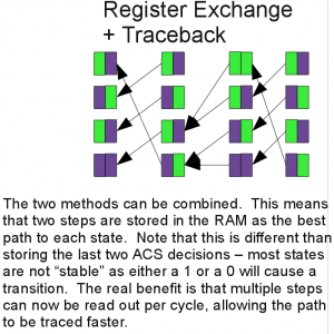
My method is a hybrid of the register-exchange and the traceback method. Instead of saving the best single-step to get to a given state, I save the best two-step path to get to that state. I thus get 256b in two cycles, which can be written 128b/cycle. This hybrid approach can be extended to larger values, but the register-exchange doesn’t scale very well. Two-steps is a good choice as it is tractable, and provides the required amount of performance. Further, it makes it easy to address the RAM.
This hybrid method has the advantage that the FPGA block rams’ mixed port widths can be used. The 2b values contain exactly the information needed, and can be easily accessed by correct addressing of the RAM. This allows the 128:1 muxes to effectively be merged into the RAMs. This comes at a cost of extra registers and 2:1 muxes on the write side which are used to implement the register exchange. In terms of implementation, I ended up using the RAMB36E1 primitives. The XST manual seemed to indicate that I couldn’t just infer the mixed-width rams. I wasn’t able to get the BRAM_SDP_MACRO to work with mixed widths — it kept getting sizing errors on internal nodes.
The traceback method does have a disadvantage that the bits are read out in reverse order. This can be corrected as a postprocessing step. It is not difficult to do using a FILO (also called a LIFO), which reads the last written element out first. I decided to make use of the SRL slices, as they have a large number of registers and a built in mux. The only issue was getting XST to actually infer them. It seems a std_logic_vector wasn’t good enough, so I created a special array type of std_logics. This method is what is shown in the dynamic shift register section of the XST guide, and did work.
The traceback unit has the longest path, and thus limits the designs clock rate. The path is simply the path from the RAM’s output back to the RAM’s address ports. This is a very simple path in terms of both logic complexity and routing. The way to make this one faster would be to use the RAM’s output register. That would only allow a valid read every other cycle, so the register exchange stage would need to be expanded to store four-step paths.


